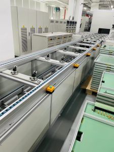
Technological advancements have increased the use of electronic devices. These gadgets have a complex internal structure to perform their functions. However, the most common component in electronics is the Printed Circuit Board. The PCB has a rigid structure to accommodate different electronic parts. PCB assembly line is the process of soldering components upon the board.
A PCB comprises-
- Fiberglass substrate
- Copper layer
- Holes to attach components
- The inner and outer layers
Let us talk about the process for the PCB assembly line.
 What are the steps for PCB assembly?
Professionals in the electronic engineering world should know about the PCB assembly line.
Use the solder paste for the board
Take the board for placing the stainless steel, thin stencil over it. Solder paste needs to be consistently and precisely applied to the circuit board. The solder mask is intended for creating a non-conducing part of the PCB. It keeps copper traces separate from each other and manages the short circuit.
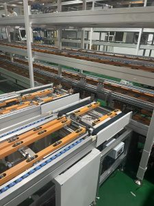
Select the machine
You need to place surface mount components on the PCB using a robotic system. Apply the soldering techniques for components on the board surface.
Solidify the solder paste
Adhere the PCB to the components by reflowing the solder paste. You can use a conveyor belt to move the PCB and its components to an oven. A temperature of around 250o C will melt the solder. The melted solder fixes the PCB parts and makes joints. After treating the PCB with a higher temperature, you have to move it to the cooler. The solder joints will undergo solidification within a short period.
 Inspect the assembly
After accomplishing the reflow process and soldering the mount components, you have to inspect the PCB. You need to test the assembled board to ensure smooth functionality. The most effective quality control processes are-
- Many designers conduct a manual inspection of the PCB assembly line to ensure the best quality.
- An automatic inspection process is better for checking a large number of PCB assemblies. Experts use an innovative optical machine and high-powered cameras to test the solder connections.
- Another option is the X-ray inspection for an intricate PCB. You can examine the PCB layers and detect potential issues.
Incorporate the through-hole component
A PTH or plated through-hole component refers to a hole in your circuit board. Instead of a simple soldering paste, you need a special soldering method for PTHs.
You may choose manual soldering for through-hole insertion. On the contrary, wave soldering is an automated process that involves molten solders for the bottom of your circuit board.
You can use a speedy chip shooter and a solder paste applier in your conveyor setup.
Final checkup
When you have soldered the PCB board assembly, conduct the final test. Run simulated signals and power to check the board’s electrical characteristics. If the PCB does not pass the test, discard it. Wash the board and dry it with compressed air.
So, these are the steps for designing your Printed Circuit Boards. When the PCB assembly line is ready, you can package it for delivery.

-768x768.jpg)