When it comes to PCB manufacturing, catching defects early is important, especially with today’s tiny components and tightly packed circuit designs. That’s why AOI is such a big deal in the SMT world. But if you’ve ever wondered, “What exactly does AOI stand for?” or “What is AOI full form?”—you’re not alone. In this blog, we’ll break down the AOI full form, explain how it works, and show you why it’s such a valuable tool in modern electronics manufacturing.
Whether you’re new to PCB design or just curious, this guide will walk you through everything you need to know, straight from the experts at SZKJ.
What is the AOI full form?
AOI stands for Automated Optical Inspection. In PCB manufacturing, this term refers to technology used to inspect printed circuit boards for defects automatically.
The process combines advanced cameras, lighting, and image processing software to examine each board with little human intervention. The goal is to ensure that every solder joint, component placement, and circuit connection meets the required quality standards.
AOI systems are designed to detect a variety of issues that could reduce the functionality or reliability of the final product. This makes them an important part of the modern SMT process.
How AOI Works
We have looked at the AOI full form, now let’s have a look at how AOI works.
The major application of AOI technology is capturing high-resolution images of the PCB and analyzing them to identify defects. The process begins with specialized cameras, which are often equipped with multiple lenses and lighting setups to highlight different features of the board.
For example, brightfield lighting is used to light up the surface uniformly, while darkfield lighting can help reveal surface defects or solder joint issues. The cameras capture detailed images of the PCB and feed them into powerful image processing software.
This software then compares the captured images against a predefined reference or standard template. It looks for discrepancies such as missing components, misaligned parts, solder bridging, cold joints, or lifted pads. The system can detect even tiny defects that are invisible to the naked eye. Once an issue is identified, the AOI system flags the defect for review or rejection, depending on the settings.
The secret to AOI’s effectiveness is its ability to analyze thousands of features rapidly and accurately. For example, it can inspect a densely populated PCB in seconds to verify that each component is placed correctly and soldered properly. Many AOI systems also use machine learning capabilities, allowing them to improve over time and adapt to new designs or components.
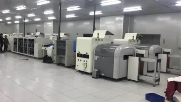
Where AOI fits in the SMT process
AOI is very useful at different stages of the SMT process, primarily before and after the reflow soldering stage.
Pre-reflow AOI inspection is performed immediately after component placement but before the heated reflow process. This step ensures that all components are correctly positioned and properly aligned before soldering. Catching errors early reduces rework and scrap, saving time and costs.
Post-reflow AOI inspection is carried out after the soldering process is complete. At this stage, the system checks for solder joint quality, component integrity, and the presence of any missing parts or bridging issues that might have occurred during reflow. This final inspection guarantees that the assembled PCB meets quality standards before it moves to the next phase of production or testing.
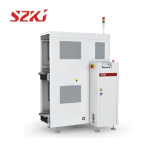
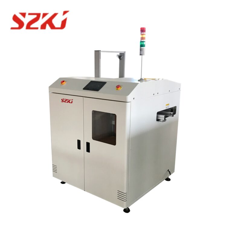
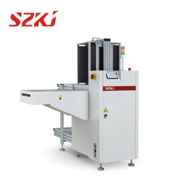
There are two main types of AOI systems used in PCB manufacturing: inline and offline. Inline AOI systems are integrated directly into the production line, inspecting each board as it moves through the assembly process. This allows for real-time detection and immediate correction of errors.
Offline AOI systems are stand-alone machines used for periodic inspection, typically for quality assurance or sampling. While offline systems may offer higher resolution or more detailed analysis, inline systems are preferred for continuous, high-volume production because of their speed and automation capabilities.
The Bottom Line
In summary, AOI, which in its full form stands for Automated Optical Inspection, is no doubt a technology that greatly improves quality control in PCB manufacturing. By automating the inspection process through advanced imaging and analysis, AOI helps detect defects early, reduce rework, and improve overall product reliability. Its integration into the SMT process—both before and after reflow—makes it indispensable for ensuring high standards in modern electronics production.
If you are looking for ways to improve your PCB inspection processes, then AOI can be just what you need. SZKJ offers cutting-edge SMT capabilities, including state-of-the-art AOI systems designed to meet the strict demands of today’s electronics industry.
We invite you to connect with us and discover how our solutions can help improve your manufacturing quality and efficiency.

-768x768.jpg)