In an era where technology permeates every facet of our lives, understanding the inner workings of electronic devices is essential. At the heart of nearly every gadget lies the PCBA—the printed circuit board assembly—bringing together components that give life to circuits and systems. In this post, we’ll unpack pcba meaning and take you through its end-to-end manufacturing journey, key applications, rigorous quality controls, and emerging trends shaping the future of electronics.
I. PCBA Fundamentals
1. PCB vs. PCBA: Definitions
PCB (Printed Circuit Board): The bare board is made of laminated copper foil, resin, and fiberglass. It provides the physical platform for electronic components.
PCBA (PCB Assembly): When the “Assembly” step transforms the PCB by mounting and soldering electronic parts (resistors, capacitors, ICs, connectors) onto it. Simply put, PCBA is a functional circuit ready for integration into a product.
2. Key Elements of a PCBA
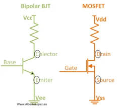
Passive Components: Resistors, capacitors, inductors—manage voltage, filter signals, and store energy.
Active Components: ICs, microcontrollers, diodes—perform processing, switching, and amplification.
Connectors & Interfaces: Headers, sockets—enable external communication and power delivery.
Example: A computer motherboard PCBA contains CPU socket, memory slots, power regulators, I/O controllers, and network interfaces, all laid out and interconnected on the board.
II. PCBA Manufacturing Process
1. Raw Material Preparation
Substrate & Copper Foil (CCL): Material selection (thickness, Tg value, copper weight) influences thermal performance, signal integrity, and mechanical strength.
Solder Mask & Silkscreen: Epoxy-based inks protect conductors and label component positions.
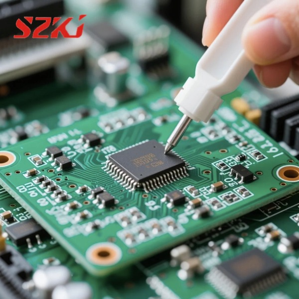
Component Procurement & Inspection: Sourcing from reliable suppliers; inspecting via optical checks, X-ray, and parameter testing to ensure defect-free parts.
2. PCB Design Phase
Schematic Capture: Defines circuit behavior and component selection.
Layout & Routing: Places parts optimally, routes traces respecting impedance, clearance, and thermal paths, often using tools like Altium or Cadence.
Design Output: Generates Gerber files, drill and pick-and-place data for fabrication and assembly.
3. PCB Fabrication
Panel Cutting & Drilling: CNC or laser drills create vias and holes to 10 µm precision.
Etching: Removes unwanted copper via controlled chemical baths after photoresist exposure.
Through-Hole Plating: Cleans hole walls, deposits copper chemically, then electroplates to form a conductive barrel from top to bottom.
Surface Finishes:
HASL (Hot Air Solder Leveling): Cost-effective, but uneven for fine-pitch parts.
OSP (Organic Solderability Preservative): Flat surface, but sensitive to handling.
ENIG (Electroless Nickel Immersion Gold): Excellent flatness and shelf life, at a higher cost.
4. PCBA Assembly
A. Surface-Mount Technology (SMT)
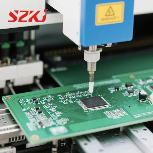
Stencil Printing: Applies solder paste at precise volumes onto pads.
Pick-and-Place: High-speed machines position components within ±20 µm accuracy.
Reflow Soldering: PCB travels through zones—preheat, soak, peak, and cool—melting paste into reliable solder joints.
B. Through-Hole Technology (THT)
Manual or Wave Soldering: Components inserted into plated holes; wave soldering bath or skilled hand soldering ensures robust joints.
C. Hybrid Assembly
Combines SMT and THT in series—SMT first, then wave solder for through-hole parts—balancing precision and mechanical strength.
5. Quality Inspection & Control
AOI (Automated Optical Inspection): Detects misalignment, missing parts post-placement.
AXI (Automated X-ray Inspection): Reveals hidden solder defects under BGAs and QFNs.
ICT (In-Circuit Test) & Flying Probe: Verifies electrical connectivity, component values, and detects shorts/opens.
Standards Compliance: Follows IPC-A-610 for solder acceptability and IPC-7711 for rework guidelines.
III. PCBA in Key Application Areas
1. Consumer Electronics
Smartphones & Tablets: Ultra-dense HDI PCBAs enabling multi-band radios, high-speed data, and miniature sensors.
Laptops: Large-area assemblies integrating power management, memory arrays, and high-speed I/O interfaces.
2. Industrial Automation
PLCs: Rugged PCBAs designed for EMI resilience, wide-temperature operation, and long MTBF.
Sensor & Drive Modules: High-precision analog front ends and power electronics on a single assembly.
3. Automotive Electronics
Engine Control Units (ECUs): PCBA designed for thermal shock, vibration, and automotive-grade reliability (AEC-Q100).
Infotainment & ADAS: High-performance graphics, camera interfaces, and real-time data fusion on complex multilayer PCBAs.
4. Medical Devices
ECG & Patient Monitors: Low-noise analog circuits, medical-grade isolation, and biocompatible assembly processes.
Ultrasound & Imaging Systems: High-speed DSP PCBAs for real-time image reconstruction.
IV. Quality Control & Reliability Assurance
1. Quality Management Systems
ISO 9001 & IPC Certifications: Frameworks ensuring consistent process documentation, training, and internal audits.
UL & CE Approvals: Safety and electromagnetic compliance are critical for global markets.
2. Reliability Testing
Environmental Stress: High-temperature bake, thermal cycling, humidity chambers.
Mechanical Stress: Vibration and shock testing per MIL-STD and automotive standards.
Electrical Stress: Power-cycling, surge, and EMC testing to guarantee field performance.
3. Continuous Improvement
Data-Driven SPC (Statistical Process Control): Tracks solder paste volume, placement accuracy, and throughput metrics.
Lean & Six Sigma: Identifies root causes of defects; implements Kaizen for yield enhancement.
Traceability: Barcodes/QR codes link each PCBA to batch data, machine settings, and inspection records.
V. Emerging PCBA Trends
1. High-Density Interconnect (HDI)
Micro-vias and buried/ blind via structures allow ever-smaller pitches, critical for ultra-thin devices.
2. 3D Packaging & Through-Silicon Vias (TSV)
Stacked die architectures reduce signal paths and enhance performance for AI and high-speed computing boards.
3. Green & Sustainable Manufacturing
Lead-Free Solder & Halogen-Free Laminates: Comply with RoHS and REACH directives.
Energy Recovery & Waste Recycling: Closed-loop solder and chemical reclamation systems reduce environmental footprint.
Conclusion
Understanding the PCBA meaning is the first step; mastering its intricate assembly processes, rigorous quality controls, and future-proof technologies is what elevates electronic manufacturing. As HDI, 3D packaging, and green initiatives redefine what’s possible, engineers and manufacturers alike must stay at the forefront, ensuring that PCBAs continue to power innovation across every industry.